Tuesday, December 22, 2009

Magnetic nanoribbons!

Owing to their nanoscale spintronic applications, doping of semiconductor nanocrystals by transition-metal ions has attracted tremendous attention . However, such doping is difficult to achieve in low-dimensional strongly quantum confined nanostructures by conventional growth procedures. In a recent report in Nature materials, researchers from korea in collaboration with american researchers have demonstrate that the incorporation of manganese ions up to 10% into CdSe quantum nanoribbons can be readily achieved by a nucleation-controlled doping process.
The cation-exchange reaction of (CdSe)13 clusters with Mn2+ ions governs the Mn2+ incorporation during the nucleation stage. This highly efficient Mn2+ doping of the CdSe quantum nanoribbons results in giant exciton Zeeman splitting with an effective g-factor of ~600, the largest value seen so far in diluted magnetic semiconductor nanocrystals. The sign of the s–d exchange is inverted to negative owing to the exceptionally strong quantum confinement in our nanoribbons. figure on the right show the theoretical investigation of Mn2+ doping of CdSe clusters.
This novel nucleation-controlled doping strategy opens the possibility of doping various strongly quantum confined nanocrystals for diverse applications.
Ref: Nature Materials 9, 47 - 53 (2009)

Thursday, December 17, 2009

Photoluminescent Silicon Quantum Dots : Chromophore for Biological Imaging


Due to their strong luminescence,Quantum dots of group II/VI such as CdSe quantum dots are well-known, and substantial research has been conducted on these systems .There have, however, been concerns over the toxicity of these quantum dots in the human body. It has been reported in past that cell damage could be caused by an uncoated CdSe core under UV excitation. Because of their low toxicity and also inexpensive nature, silicon nanoparticles emerges as an ideal candidate for biological fluorescence imaging. In a recent article in JACS, researchers from New Zealand and Japan suggested the synthesis of amino-terminated silicon quantum dots made in reverse micelle system and capped with allylamine using a platinum catalyst. Their newly developed technique of surface modification is multistepped based on the chemistry of the terminal double bond on the surface to achieve the target functionalities. Thus formed Silicon quantum dots were characterized by transmission electron microscopy (TEM) and energy dispersive spectrometry (EDS). The capping of the silicon quantum dots has been fully characterized using nuclear magnetic resonance (NMR) and Fourier transform infrared spectroscopy (FTIR). The results from cytotoxicity studies indicate that toxicity is dependent on the surface functionality and that the silicon quantum dots as prepared have potential in biological applications such as bioimaging. In summary, silicon quantum dots opens new doors in the field of biological imaging.
Ref:
J. Am. Chem. Soc., Article ASAP, DOI: 10.1021/ja906501v

Monday, December 14, 2009

Single Molecule detection by SERS active Gold-Silver-Core-Shell Nanodumbbells

Detection methods using plasmonic nanostructures based on Surface-enhanced Raman scattering (SERS) have been widely investigated for imaging and sensing applications.However, SERS-based single-molecule detection generally faces a problem with structural reproducibility, as particle structure and interparticle distance can markedly affect Raman signals and constructing robust SERS-active nanostructures still remain a challenge.
Recently, in a article in Nature Materials, researchers have reported a high-yield synthetic strategy to obtain gap-tailorable gold–silver core–shell nanodumbbells (GSNDs) and subsequent hot SERS-based single-molecule detection with structurally reproducible dimetric nanostructures.
Gold nanoparticle heterodimers were successfully synthesized in a relatively high yield by means of a single-target-DNA hybridization (displayed in the figure). A single Raman-active Cy3 dye molecule is located between two DNA-tethered particles. In another step, Ag shells were formed on the surface of the dimeric Au nanoparticles, and the Ag shell thickness was controlled on the nanometre scale to generate gap-engineerable, DNA-embedded GSNDs. To detect a Raman signal from each single-DNA-captured GSND, atomic force microscope (AFM)-coupled nano-Raman spectroscopy was used.
To prove that single-DNA detection is possible from a single GSND structure, several characterization experiments were suggested in the article.It has been demonstrated that as formed Raman-active GSNDs have single-molecule sensitivity with high structural reproducibility. This research is important because of following reasons:
- opens new opportunities in the high-yield synthesis of specific nanostructures for materials science and bio-detection applications..
- unlike the conventional strong electrolyte-induced nonspecific nanoparticle aggregation, this synthesis method can be easily scalable to produce targeted SERS-active nanoprobes.
- the nanogap-engineering of GSNDs allows for exploring hot SERS structures in an efficient and straightforward fashion
To summarize, these SERS-active GSNDs could be further modified by other biomolecules (such as proteins) and used as both in vitroand in vivo bio-labelling probes with ultrahigh sensitivity, quantification potential and multiplexing capability.
reference: Nature Materials (13 December 2009) doi:10.1038/nmat2596

Thursday, December 10, 2009

Flexible Floating-gate Transistor


Traditionally, high-temperature manufacturing methods are employed for fabricated electronic device using inorganic semiconductors and rigid substrates . Organic semiconductors on the other hand can be processed at low temperatures and on large-area polymeric substrates. This has allowed for the development of a variety of electronic devices on flexible plastic substrates, including solar cells.Most of the organic memory transistors reported to date exploit the electric field–induced remnant polarization in ferroelectric polymer films . A considerable limitation of ferroelectric polymer memory transistors is that the coercive field required to reverse the macroscopic polarization increases with decreasing film thickness, which makes it difficult to obtain a large enough memory window with program and erase voltages below about 20 V. Also, due to the substantial surface roughness of the ferroelectric polymer films, the carrier field-effect mobility in these transistors is usually quite low.
Although silicon floating-gate transistors are excellent for high-density data storage, flexible organic floating-gate transistors are potentially useful for large-area sensors and actuators with integrated nonvolatile memory capability.
Using organic transistors with a floating gate embedded in hybrid dielectrics that comprise a 2-nanometer-thick molecular self-assembled monolayer and a 4-nanometer-thick plasma-grown metal oxide, nonvolatile memory arrays on flexible plastic substrates is realized . The small thickness of the dielectrics allows very small program and erase voltages (≤6 volts) to produce a large, nonvolatile, reversible threshold-voltage shift. The transistors endure more than 1000 program and erase cycles, which is within two orders of magnitude of silicon-based floating-gate transistors widely employed in flash memory. By integrating a flexible array of organic floating-gate transistors with a pressure-sensitive rubber sheet, a sensor matrix that detects the spatial distribution of applied mechanical pressure and stores the analog sensor input as a two-dimensional image over long periods of time has been created.
Ref: Science
11 December 2009: Vol. 326. no. 5959, pp. 1516 - 1519

Wednesday, December 9, 2009

Bamboo like Carbon Nanorods fabricated by Non-catalytic Approach

Since their discovery in 1990s, Carbon nanotubes (CNTs) are continuously of great interest in both fundamental research and practical applications. As an important member of carbon material family, bamboo-like carbon nanotubes (BCNTs) have been explored extensively due to their unique properties resulting from their hollow compartments inside nanotubes. BCNTs are expected to exhibit excellent electrochemical performances for their high percentage of edge sites along inner wall, compared with the common straight CNTs. For there synthesis, the catalyst is usually used and left inside the final carbon nanotubes, which needs further purification before their applications.
A novel approach for non-catalytic fabrication of BCNT has been suggested by Scientist from China in their recent article in Material Letters. The preparation procedures involve synthesis of monodispersed core–shell structured polymer spheres and the pyrolysis in an argon atmosphere.

The carbon nanotubes with bamboo-like structures are formed via the pyrolysis of PMMA@PDVB core–shell structured spheres. The typical SEM image reveals the one dimensional (1D) twisted nanostructures of BCNTs, which are up to several tens of micrometers in length. The compartments inside the nanotubes are observed from representative TEM images. The wall thickness of the BCNTs is between 20 and 30 nm and the inner diameter is around 200 nm. High-resolution TEM image reveals the lattice fringes with the space of 0.357 nm, which corresponds with the (002) plane lattice parameter of graphitic carbon. X-ray powder diffraction (XRD), Raman spectroscopy and energy dispersive spectroscopy (EDS) measurements were performed to get insight into the structure of BCNTs. Also, the possible mechanism for fabrication has been proposed in the report.

Monday, December 7, 2009

Platinum nanoparticles: Converting homogeneous to heterogeneous catalysis

Uniting the advantages of homogeneous and heterogeneous catalytic processes is a continuing goal in the field of catalysis.
Nanoparticles represent a new frontier in heterogeneous catalysis, where this unification can also be supplemented by the ability to obtain new or divergent reactivity and selectivity. Researchers at University of Berkeley, California reported a novel method for applying heterogeneous catalysts to known homogeneous catalytic reactions through the design and synthesis of electrophilic platinum nanoparticles.
These nanoparticles are selectively oxidized by the hypervalent iodine species PhICl2, and catalyse a range of π-bond activation reactions previously only catalysed through homogeneous processes. Multiple experimental methods are used to unambiguously verify the heterogeneity of the catalytic process. The discovery of treatments for nanoparticles that induce the desired homogeneous catalytic activity should lead to the further development of reactions previously inaccessible in heterogeneous catalysis. Furthermore, a size and capping agent study revealed that Pt PAMAM dendrimer-capped nanoparticles demonstrate superior activity and recyclability compared with larger, polymer-capped analogues.
reference : Nat. Chem., DOI: 10.1038/nchem.468

Saturday, December 5, 2009

Nanodome Solar Cells with High Efficiency!


Solar cells of nanostructures such as nanocrystals and nanowires have attracted much attention due to their potential for improving charge collection efficiency, fabricating small-scale power sources, enabling novel conversion mechanisms, and using low-cost processes.
Recently in a Nano letters report, Researchers at Stanford University have demonstrate novel nanodome solar cells, which have periodic nanoscale modulation for all layers from the bottom substrate, through the active absorber to the top transparent contact. These devices combine many nanophotonic effects to both efficiently reduce reflection and enhance absorption over a broad spectral range.
Nanodome solar cells with only a 280 nm thick hydrogenated amorphous silicon (a-Si:H) layer can absorb 94% of the light with wavelengths of 400−800 nm, significantly higher than the 65% absorption of flat film devices. Because of the nearly complete absorption, a very large short-circuit current of 17.5 mA/cm2 is achieved in our nanodome devices. Excitingly, the light management effects remain efficient over a wide range of incident angles, favorable for real environments with significant diffuse sunlight. Nanodome devices demonstrated with a power efficiency of 5.9%, which is 25% higher than the flat film control. The nanodome structure is not in principle limited to any specific material system and its fabrication is compatible with most solar manufacturing; hence it opens up exciting opportunities for a variety of photovoltaic devices to further improve performance, reduce materials usage, and relieve elemental abundance limitations.
Also, these nanodome devices when modified with hydrophobic molecules present a nearly superhydrophobic surface and thus enable self-cleaning solar cells.

Wednesday, December 2, 2009

Mistery of Crystallization


For many years scientists have scratched surfaces to promote crystallization. Crystals are observed to nucleate along the scratches. Despite the popularity of this technique, our understanding of why crystals nucleate in scratches is very limited. There have been no quantitative measurements of the nucleation rate in a groove, and there is no data on the microscopic details of how the nucleation occurs here.
In a recent report in JACS, Researcher from U.K. studied the heterogeneous nucleation of a crystal in a wedge-shaped groove via computer simulation.They found that nucleation in these grooves is indeed many orders of magnitude faster than on a flat surface. It is also been found that there is a competition between the angle of the wedge, and the angles that are intrinsic to the lattice of the crystal. This competition results in a wedge angle at which the nucleation rate goes through a maximum, a phenomenon that is not seen in the nucleation of liquids.
Therefore, generically we expect crystallization to start in grooves or pits in surfaces, not on the flat parts of surfaces. This expectation is consistent with the common observation that crystallization readily occurs on a scratched surface. It been found that nucleation is highly sensitive to the wedge angle β. This is because there are angles that are intrinsic to crystals, such as the 70.5° angle between the close-packed planes in an fcc lattice. As this effect is a direct consequence of the crystal lattice it has been expected to be a general feature of crystallization, even with more complex molecules, for example proteins. Nucleation is faster when the wedge angle is such that a defect-free unstrained piece of the crystal fits perfectly into the wedge. As different crystal polymorphs have different intrinsic angles, this may provide a way to control the polymorph that nucleates. A wedge into which the desired polymorph fits perfectly, but which has the wrong angle for other polymorphs, will favor nucleation only of the desired polymorph.

Reference : J. Am. Chem. Soc., 2009, 131 (48), pp 17550–17551

Tuesday, December 1, 2009

Nanoplasmonic Probes of Catalytic Reactions


Scientists from Sweden have recently published a report in Science, which discuss about their newly developed plasmonic sensing method for heterogeneous catalytic reactions based on arrays of nanofabricated gold disks, covered by a thin (~10 nanometer) coating (catalyst support) on which the catalyst nanoparticles are deposited.
In heterogeneous catalysis, reactants in gas or liquid phase are converted to desired product molecules on the surface of a solid catalyst, which is usually composed of catalytically active nanoparticles (1 to 10 nm) dispersed on a porous, high-surface-area support material. In order to understand and improve these systems, it is important to be able to monitor the catalyst’s state and to follow the reaction in real time. An important quantity is the surface coverage of reactants. However, experimental difficulties arise from the complexity of the catalyst and the atmospheric or higher pressures in which the reactions occur. Model systems (commonly single-crystal surfaces) and model reactions are frequently investigated at idealized ultrahigh vacuum (UHV) conditions, allowing use of powerful experimental probes (such as electrons, photons, or ions). A major challenge is to correlate results obtained by using the idealized and thoroughly scrutinized model catalysts in UHV with those of the less characterized real nanostructured catalysts at real reaction conditions.


This Report describe a method that, with a simple optical transmission (or reflection) measurement, can follow catalytic reactions in real time for both model and real supported catalysts. The principle is "nanoplasmonic" [localized surface plasmon resonance (LSPR)] sensing, currently intensely explored for biosensing, down toward single-molecule sensitivity. It is shown that LSPR can monitor changes in adsorbate coverages on "realistic" supported catalysts with a sensitivity corresponding to much less than 0.1 monolayer (ML).
The LSPR sensing structures are nanoscale disks of gold or platinum. The light transmitted through the sample has an intensity minimum (maximum extinction) at the wavelength at which the LSPR excitation in the sensing particles is strongest. The excitation creates a strongly enhanced electromagnetic near field, which acts as a probe of the nanoparticle’s surrounding.
For detailed experimental study please goto Science, Vol. 326. no. 5956, pp. 1091 - 1094

Saturday, November 28, 2009

Gold based Nanocages and Nanoboxes: Effective Catalysts for Redox Reaction
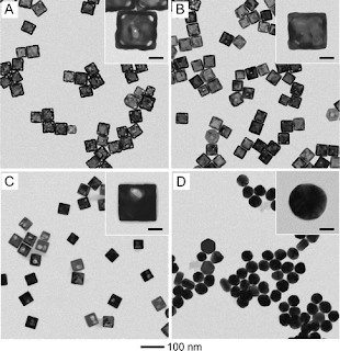

Scientists from Korea in collaboration with scientist at washington University, Missouri recently evaluated the catalytic properties of Au-based nanostructures (including nanocages, nanoboxes, and solid nanoparticles) using a model reaction based on the reduction of p-nitrophenol by NaBH4
.
It is well-known that the catalytic activity of a nanoparticle is strongly dependent on its size. Typically, a smaller nanoparticle tends to show a higher catalytic activity as it has a much greater surface-to-volume ratio.However, smaller nanoparticles may not be better candidates for catalyzing all types of reactions. A good example for explaining this exception can be found in a redox reaction. As the catalytic particles become increasingly smaller, the oxidation and reduction half reactions might need to occur on different particles due to the reduction in surface area. In this case, a good “electrical” connection between the particles will play an important role as the electrons have to be transported from the site of oxidation to the site of reduction. The redox reaction will be unable to proceed if the catalytic particles are separated from each other by an insulating medium.It has been argued that this kind of problem can be solved by switching from solid nanoparticles to nanocages or nanoboxes with hollow interiors and ultrathin walls. For a Au-based nanocage of 50 nm in edge length and 5 nm in wall thickness, it should be able to provide a sufficiently large surface area (at least, equivalent to a 50 nm solid particle) to accommodate both the oxidation and reduction half reactions while the ultrathin wall is still able to provide a high activity equivalent to a 5 nm solid particle due to a good electrical connection across the entire surface of the wall. For a model reaction based on the reduction of p-nitrophenol by sodium borohydride (NaBH4), The experimental data reported indicate that both wall thickness and porosity of the Au-based hollow nanostructures play an important role in enhancing the catalytic activity. The kinetic data in their report (published in Nano letters) indicate that the Au-based nanocages are catalytically more active than both the nanoboxes and nanoparticles probably due to their extremely thin but electrically continuous walls, the high content of Au, and the accessibility of both inner and outer surfaces through the pores in the walls.
In summary, the good intrinsic electrical connection across the entire surface of a Au nanocage makes it a much better catalyst than small Au solid nanoparticles for a redox reaction. In addition, a typical compensation effect was observed in this catalytic system, which can be explained by the assumption of kinetic regime switching. Given the high abundance of Au element relative to other noble metals like Pt and Pd as well as the easiness in controlling the porosity and morphology, the Au-based nanocages might be able to find widespread use as catalysts in a number of industrial applications.

India's ambitious 'Solar Mission'

India's prime minister Manmohan Singh has approved a US$19 billion plan to make the country a global leader in solar energy over the next three decades. The ambitious project would see a massive expansion in installed solar capacity, and aims to reduce the price of electricity generated from solar energy to match that from fossil fuels by 2030.

The 'solar mission' was first mooted as part of India's national action plan on climate change, announced in June 2008. According to a draft mission document whose targets were approved on 3 August, installed solar capacity would be hiked from its current 5 MW to 20 GW by 2020, 100 GW by 2030 and 200 GW by 2050 — more than the current 150 GW power generation capacity of all India's coal, gas and nuclear plants.

Officials say the plan shows that the country is serious about its intention to stem global warming, ahead of the UN climate change conference in Copenhagen in December.

A detailed road map has been drawn up to 2020. By then, according to the mission document, solar lighting will be available for 20 million households and 42 million tonnes of CO2 emissions will be saved annually by the switch to solar energy. The government plans to create a solar fund with initial investment of $1.1 billion and build it up by taxing fossil fuels and the power generated from them — 0.1 cents for every kWh produced. By 2030, it hopes to reduce the cost of electricity from photovoltaic cells to around 10 cents per kWh, matching the price of electricity derived from conventional fuels.

The plan will be pushed forward by a mixture of other policy and regulatory measures. Those include making it mandatory for existing thermal power plants to generate at least 5% of their capacity from solar power, and for government buildings to install photovoltaic panels on rooftops. Producers connected to the grid will be able to sell their excess solar electricity to utilities; solar-power projects get a 10-year tax holiday; and other 'carrots' for the industry include the duty-free import of raw materials and priority bank loans.

An autonomous solar-energy authority will be created to execute the mission, but the existing solar-energy centre near New Delhi will be upgraded into an 'apex research institute' to coordinate solar-research centres across the country and promote foreign collaboration. The mission document recommends introducing solar-energy courses to the Indian Institutes of Technology, and creating a fellowship programme to train 100 Indian scientists a year in world-class institution


Tuesday, November 24, 2009

Developing Complex Patterns on Surface

Researchers at Worcester Polytechnic Institute, Worcester, Massachusetts have recently published an interesting report in Langmuir. They have develop a method for developing complex nanopatterns on surfaces by combining self-assembly, photolabile protecting groups, and multilayered films. An o-nitrobenzyl protecting group has been incorporated into molecular level films utilizing thiol-gold interactions. When the o-nitrobenzyl group is cleaved by ultraviolet light, a carboxylic acid terminated layer remains on the surface and is available for activation and further functionalization through amide bond formation. Using this method, multilayered films have been constructed and characterized by contact angle goniometry, cyclic voltammetry, grazing incidence infrared spectroscopy, and X-ray photoelectron spectroscopy measurements. Complex surface patterns can be achieved by creating a surface array using a photomask and then further fictionalizing the irradiated area through covalent coupling. Fluorophores were attached to the deprotected regions, providing visual evidence of surface patterning using fluorescence microscopy. Their approach is universal to bind moieties containing free amine groups at defined regions across a surface, allowing for the development of films with complex chemical and physicochemical properties.
Figure. Fluorescence microscopy images of surfaces patterned with 100 μm squares (top) and 100 μm lines separated by 150 μm spaces (bottom), images on the left are of rhodamine 110 (green) and images on the right are cresyl violet 670 (red). Inset: reduced scale images of the photomasks used to pattern the surfaces.

Monday, November 23, 2009

Biomedical Imaging of Cells using Quantum Dots

A joint research team, working at the National Institute of Standards and Technology (NIST) and the National Institute of Allergy and Infectious Diseases (NIAID), has discovered a method of using nanoparticles to illuminate the cellular interior to reveal these slow processes. Nanoparticles, thousands of times smaller than a cell, have a variety of applications. One type of nanoparticle called a quantum dot glows when exposed to light. These semiconductor particles can be coated with organic materials, which are tailored to be attracted to specific proteins within the part of a cell a scientist wishes to examine.

These quantum dots last longer than most of the organic dyes and fluorescent proteins that we previously used to illuminate the interiors of cells. They also have the advantage of monitoring changes in cellular processes while most high-resolution techniques like electron microscopy only provide images of cellular processes frozen at one moment. Using quantum dots, cellular processes involving the dynamic motions of proteins can be elucidated.

In the recent study, the research team focused primarily on characterizing quantum dot properties, contrasting them with other imaging techniques. In one example, they employed quantum dots designed to target a specific type of human red blood cell protein that forms part of a network structure in the cell's inner membrane. When these proteins cluster together in a healthy cell, the network provides mechanical flexibility to the cell so it can squeeze through narrow capillaries and other tight spaces. But when the cell gets infected with the malaria parasite, the structure of the network protein changes.

Since the clustering mechanism is not well understood, it was examined with the dots. Researchers believed that if they could develop a technique to visualize the clustering, they could learn something about the progress of a malaria infection, which has several distinct developmental stage.


fig : Human red blood cells, in which membrane proteins are targeted and labeled with quantum dots, reveal the clustering behavior of the proteins. The number of purple features, which indicate the nuclei of malaria parasites, increases as malaria development progresses. The NIST logo at bottom was made by a photo lithography technique on a thin film of quantum dots, taking advantage of the property that clustered dots exhibit increased photoluminescence. (White bars: 1 micrometer; red: 10 micrometer)

The team's efforts revealed that as the membrane proteins bunch up, the quantum dots attached to them are induced to cluster themselves and glow more brightly, permitting scientists to watch as the clustering of proteins progresses. More broadly, the team found that when quantum dots attach themselves to other nanomaterials, the dots' optical properties change in unique ways in each case. They also found evidence that quantum dot optical properties are altered as the nanoscale environment changes, offering greater possibility of using quantum dots to sense the local biochemical environment inside cells. about the progress of a malaria infection, which has several distinct developmental stages.


Saturday, November 21, 2009

Nanostructured Integrated Circuits detect Type and Severity of Cancer

The analysis of panels of nucleic acid biomarkers offers valuable diagnostic and prognostic information for cancer management. Scientists at University of Toronto published a recent article in ACSNano where they reported a chip onto which they integrated novel nanostructured microelectrodes and with which direct detection of cancer biomarkers in heterogeneous biological samples—both cell extracts and tumor tissues is possible. Coarse photolithographic microfabrication defines a multiplexed sensing array; bottom-up fabrication of nanostructured microelectrodes then provides sensing elements. They have analyzed a panel of mRNA samples for prostate cancer related gene fusions using the chip. Gene fusions were identified which can correlate with aggressive prostate cancer and distinguished these from fusions associated with slower-progressing forms of the disease.
The multiplexed nanostructured microelectrode integrated circuit reported provides direct, amplification-free, sample-to-answer in under 1 h using the 10 ng of mRNA readily available in biopsy samples. The detection platform described in this research is not only specific, sensitive, and robust, but it is also practical and scalable. The reproducible fabrication method chosen is amenable to the production of probe-modified chips using the same photolithographic technologies in widespread use in consumer electronics microchip fabrication, and only simple, inexpensive instrumentation is needed for readout. Microfluidics are not required for automated analysis, as hybridization can be performed and read out in a single reaction vessel. This system represents an attractive alternative to PCR-based methods that are sensitive but difficult to automate in a clinical setting.
In summary, the new multiplexed electrode platform suggested in the paper is the first to read directly a panel of cancer biomarkers in clinically relevant samples using electronic signals. The array enabling these measurements features microelectrodes that possess controllable and versatile nanotexturing essential for sensitivity. The system combines these nanotextured electrodes with rapid catalytic readout to achieve a long-standing goal: the multiplexed analysis of cancer biomarkers using an inexpensive and practical platform.

Friday, November 20, 2009

Direct Imaging in Real Space and Time with 4D Electron Microscopy
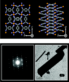
The current methods of detection of nano structures provide insight into the movements but direct real-space and time visualization of modes of oscillations at frequencies pitched in the ultrasonic range (i.e., kilohertz to gigahertz) has not so far been possible.Scientist at Caltech (Ahmed H. Zewail et al), for the first time have reported their observation using four-dimensional (4D) electron microscopy, of the nanomechanical motions of cantilevers.
From the observed oscillations of nanometer displacements as a function of time, for free-standing beams, They were able to measure the frequency of modes of motion and determine Young’s elastic modulus and the force and energy stored during the optomechanical expansions. The motion of the cantilever is triggered by molecular charge redistribution as the material, single-crystal organic semiconductor, switches from the equilibrium to the expanded structure. For these material structures, the expansion is colossal, typically reaching the micrometer scale, the modulus is 2 GPa, the force is 600 μN, and the energy is 200 pJ. These values translate to a large optomechanical efficiency (minimum of 1% and up to 10% or more) and a pressure of nearly 1,500 atm. This has been noted that the observables in the report are real material changes in time, in contrast to those based on changes of optical/contrast intensity or diffraction. The pseudo-one-dimensional molecular material (copper 7,7,8,8-tetracyanoquinodimethane, [Cu(TCNQ)]), which forms single crystals of nanometer and micrometer length scale, has been used as a prototype.Figure show the Atomic scale to macroscale structure of phase I Cu(TCNQ). Shown in the upper panel is the crystal structure as viewed along the a axis (i.e., π stacking axis) and c axis. The unit cell is essentially tetragonal, gray corresponds to carbon, blue corresponds to nitrogen, and yellow corresponds to copper. The lower panel displays a typical selected-area diffraction pattern from Cu(TCNQ) single crystals as viewed down the [011] zone axis along with a micrograph taken in our UEM. The rodlike crystal habit characteristic of phase I Cu(TCNQ) is clearly visible.
In summary, researchers have successfully suggested that with 4D electron microscopy it is possible to visualize in real space and time the functional nanomechanical motions of cantilevers. From tomographic tilt series of images, the crystalline beam stands on the substrate as defined by the polar and azimuthal angles. The resonance oscillations of two beams, micro- and nanocantilevers, were observed in situ giving Young’s elastic modulus, the force, and the potential energy stored. The systems studied are unique 1D molecular structures, which provide anisotropic and colossal expansions. The cantilever motions are fundamentally of two types, longitudinal and transverse, and have resonance Q factors that make them persist for up to a millisecond. The function is robust, at least for 107 continuous pulse cycles (1011 oscillations for the recorded frames), with no damage or plasticity. With these imaging methods in real time, and with other variants, it will be now possible to test the various theoretical models involved in MEMS and NEMS.

Thursday, November 19, 2009

Ultraflat Graphene
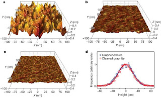

Graphene, a single atomic layer of carbon connected by sp2 hybridized bonds, has attracted intense scientific interest since its recent discovery. Much of the research on graphene has been directed towards exploration of its novel electronic properties, but the structural aspects of this model two-dimensional system are also of great interest and importance.
Detailed electron-diffraction studies of free-standing graphene monolayers indicate the presence of an intrinsic rippling, with 1-nm-high corrugations normal to the surface appearing over a characteristic lateral scale of 10–25 nm. It has been argued that these corrugations are necessary to stabilize the suspended graphene sheets against thermal instabilities present in ideal two-dimensional systems.
Researchers from University of Columbia have recented published a report in Nature,where they report the fabrication and characterization of high-quality ultraflat graphene monolayers by making use of a mica support that provides atomically flat terraces over large areas. Using high-resolution, non-contact mode atomic force microscopy (AFM) to characterize the morphology, They have found that graphene on mica approaches the limit of atomic flatness. The availability of such a flat substance provides insight into questions of thermodynamic stability for this model two-dimensional system and also a reference material with which to determine the role of ripples in the panoply of observed and predicted phenomena.
Their measurements demonstrate unambiguously that intrinsic ripples in graphene, if they do exist, can be strongly suppressed by interfacial van der Waals interactions when this material is supported on an appropriate atomically flat substrate.